AlScN Ferroelectric Junctions
Device research · cryogenic memory · compute-in-memory
Ultrathin all-nitride ferroelectric junctions, 1 nm AlN / 4 nm AlScN / 1 nm AlN between aluminum electrodes, measured from 400 down to 14 K in Penn’s Device Research and Engineering Laboratory. I run the measurements and write the analysis; the group’s results are below. The paper itself is a manuscript in preparation and is not public yet.
Overview
Aluminum scandium nitride (AlScN) is a wurtzite nitride ferroelectric with strong polarization, thermal stability, and sputter-based back-end-of-line compatibility. This work studies monolithic all-nitride Al / AlN / AlScN / AlN / Al junctions built around a 1 nm AlN / 4 nm AlScN / 1 nm AlN active stack, and asks whether a 6 nm heterostructure can preserve ferroelectric switching and a nonvolatile resistance readout from elevated temperature down to cryogenic operation.
What I did
- Operated the cryogenic and high-temperature probe stations for the device measurements.
- Ran the DC and AC J–V, C–V, PUND, breakdown and endurance measurements used in the analysis, and wrote the measurement sequences so every device and temperature point is captured the same way.
- Collected and organized the temperature-dependent characterization data.
- Analyzed switching, hysteresis, breakdown, capacitance, polarization, endurance, ON/OFF ratio and read-current trends across temperature.
- Wrote the Python for data processing, visualization, parameter extraction and device-to-device comparison.
- Built the device visuals: the cross-section in Fig. 2, and 3D CAD models of the device stack and of an 8 × 8 crossbar array for the compute-in-memory work.
What I measure
| Measurement | Sweep | What I extract from it |
|---|---|---|
| J–V | DC and AC | Switching voltages, the ON/OFF current ratio, and the read current after each switch |
| C–V | AC | The capacitance loop against bias, and where its peaks sit |
| PUND | Pulse train | Switched polarization, separated from leakage and capacitive current |
| Breakdown | Ramped field | The breakdown field |
| Endurance | Repeated cycles | How the switching window holds up over repeated cycles |
Every measurement is repeated across the 14 to 400 K range, on a cryogenic station at the low end and a high-temperature station at the top, so the same device can be compared with itself across temperature.
What we found
| Quantity | Value | Condition |
|---|---|---|
| Ferroelectric switching | 400 to 14 K | Hysteretic switching preserved across the whole range in the 6 nm junction |
| ON/OFF ratio | > 2 | Across the measured temperature range |
| Coercive field | ≈ 5.4 MV/cm | At 14 K |
| Breakdown field | ≈ 11.5 MV/cm | Under 10 kHz operation |
Temperature- and field-dependent transport point to a tunnel-dominant, local trap-assisted readout mechanism, rather than direct tunneling through the full stack or classical Poole–Frenkel emission alone.
Compute-in-memory
Beyond binary memory, the measured conductance states serve as programmable analog weights for vector-matrix multiplication. Multilevel conductance programming made possible a repetition-code syndrome decoder, built from measured devices, for detecting and decoding qubit errors. Together with the cryogenic operation, that points to scaled all-nitride ferroelectric junctions as candidates for memory and local compute next to quantum-control hardware.
Device models
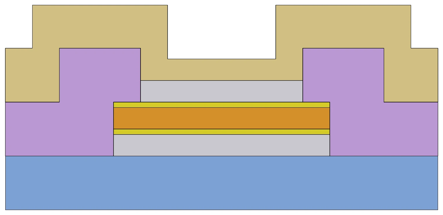
I also built 3D CAD models of the device stack and of an 8 × 8 crossbar array of these junctions, for the compute-in-memory work.
Paper
The results above are from a manuscript in preparation, to which I contributed measurements and analysis. The paper, its figures and its data stay private until it is published; it will be linked here then.